“It was difficult to implement complementary logic circuits with conventional two-dimensional semiconductor devices because they only exhibit the characteristics of either n-type or p-type devices due to Fermi-level pinning,” according to NIST. In contrast, with the new electrode, “it is possible to freely control the characteristics of the n-type and p-type devices by minimising defects with the semiconductor interface. In other words, a single device performs the functions of both n-type and p-type devices.”
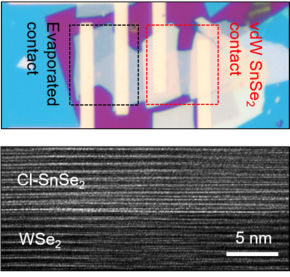
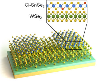
The 2D semiconductor in question is tungsten diselenide (WSe2), whose transistors exhibit n-type transport when evaporated metal contacts are used and, thanks to the KIST work, p-type transport when 2D metallic Cl-SnSe2 contacts are used, as its high work-function provides an interface that is free of defects and Fermi-level pinning.
“Such clean contacts can pose nearly ideal Schottky barrier heights, following the Schottky–Mott limit and thus permitting polarity-controllable transistors,” according to ‘Fermi-level pinning-free WSe2 transistors via 2D Van der Waals metal contacts and their circuits’, a paper published on the work in Advanced Materials.
Clean here is emphasised because pinning is mostly attributed to chemical and physical damage to the 2D semiconductor when conventional electrode metallisation is used, and the pinning fixes the Schottky barrier, usually in a way which makes an n-type transistor, according to the team.
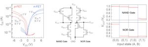
NOR and NAND gates were made using the 2D CMOS
“The developed two-dimensional electrode material is very thin, hence they exhibit high light transmittance and flexibility. Therefore, they can be used for next-generation flexible and transparent semiconductor devices,” added KIST researcher Do Kyung Hwang, who worked with Professor Kimoon Lee of Kunsan National University.
‘Fermi-level pinning-free WSe2 transistors via 2D Van der Waals metal contacts and their circuits‘ is extensive and clearly-written. It can be read in full through Advanced Materials without payment.
"type" - Google News
May 30, 2022 at 09:11PM
https://ift.tt/SrOlWHw
p-type 2D transistors mean atomically-thin CMOS is not far away - Electronics Weekly
"type" - Google News
https://ift.tt/cFC3eiq
https://ift.tt/qi6o5tE
Bagikan Berita Ini


0 Response to "p-type 2D transistors mean atomically-thin CMOS is not far away - Electronics Weekly"
Post a Comment